
We had a two year long project to decommission our Summa Four switches. It wasn’t supposed to be a two year long project, but the goal was to transition from traditional telephony backends to VoIP without needing to touch any of our existing applications. My team maintained EOS, the runtime system for the applications, so the bulk of the work was ours. The existing applications numbered in the thousands (some over 20 years old), so testing continually surfaced additional requirements. So, hundreds of bug reports and 2 years later, we were done and the decommissioning party we had been promised was long forgotten.
Time passes.
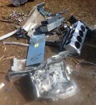
Then last May we were doing additional data center cleanup and our very last Summa was pulled out to be recycled. Desire for a proper decommissioning arose from the ranks and new management was more than happy to oblige with a party not to be forgotten. As a sort of team building exercise and to take out aggression against the Summa (and whatever recent projects may have had people stressed) we loaded up the Summa and two legacy VRU servers and headed out into rural Nebraska, guns, ammo, and pounds of tannerite in tow.
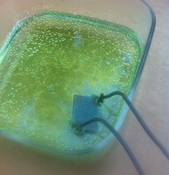
EOS. GO. BOOM! Two EOS units are sitting on top of the Summa cabinet about in the middle of the screen.
Catharsis
After
some amount of cleanup we were left with just jagged remains of the
servers that had tormented us so much. To carry us through the crazy
deadlines and insane projects ahead, many of us took pieces or gnarled
metal and twisted wires to keep at our desks to remind us who is in
charge. That’s right Summa… we are. I took the front face plate of
what once was eos689. It ran SCO, so I’m pretty sure it’s in hell now.
Or at least it WAS! Mwah ha DUM! (I couldn’t decide if “Mwah ha ha ha” or “DUM DUM DUM!” was more apropos)
Being the fan of zombies that I am, I couldn’t resist creating an undead effigy of the EOS that once was. My goal was to make the face plate appear to still be a functional server, with a lit power light, flashing error lights, and a periodically busy HDD light. That makes the cubicle ornament a little more of a conversation piece as well.
The Undead EOS
Initially I was debating between just making the undead server look like it was working and trying to make it a fully functional server, perhaps by mounting a Raspberry Pi to the back. Once you add the processor and all the bits you need to connect it to a network and power it there would be no hiding that the it had been modified from the original. After about a week flip-flopping between the art of a seemingly unmodified partial server with blinky lights and the cool factor of a functioning system, I opted in favor of art.
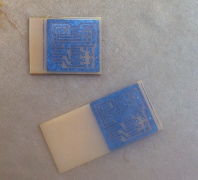
So how could I make the lights blink without obvious additional circuitry hanging off the back? The chassis has a small daughter board bolted to the front panel that has the LEDs and two reset switches mounted on it. Between that circuit board and the frame there is normally about 1/4 inch of space, but due to a bend in the face plate (a direct result of a recent explosion), the gap was as narrow as 1/8 near the middle. There was plenty of real estate behind the daughter board, but the components would need to be very low profile. Enter SMD (Surface Mount Device). Unlike their DIP (dual inline package) cousins, SMD mount directly on the circuit board rather than having pins that protrude through it. That and their smaller size make them fit the bill.
Circuit Design
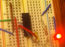
I
started by bread boarding out some options for the circuit using
regular DIP integrated circuits. I planned on using a 555 Timer to
produce a pulse and a counter IC to produce different on-off patterns
for the LEDs. Originally I played around with decade counters, put
quickly landed on a binary counter (CD4024).
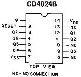
The pinout of the CD4024 has pins Q1-Q7 which are essentially the bits of a 7-bit number. Each pulse from the timer increments the number, so the low order bit Q1 will turn on and off in step with the pulse. Q2 will turn on and off half as fast, etc.. I wired what would be the error LEDs to Q4, for about a 1/2 second blink (1/4s on – 1/4s off). I wanted the HDD light to be pseudo-random to look like real hard drive activity. That meant I wanted some periods of rapid blinking and some slower. To accomplish that I shorted together several of the other Q pins. Q3,Q6 and Q7 as the anode side of the LED and Q1 as the cathode resulted in a pattern that was suitably HDD looking. Being a bit of an off-spec usage of the IC I found that the manufacturer of the IC mattered as far as the behavior. My DIP IC was a TI, so I needed to track down the same TI chip in a SMD package. (Thanks Digi-Key, also thanks to Mouser while I’m at it.)
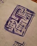
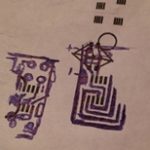
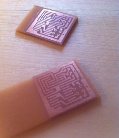
Next I needed to work on the layout of the circuit to get everything wired together properly on a single layer of traces. I worked out the design on paper whenever I was bored. Although a small wire jumper here or there would have been quicker, it was fun exercising a little lateral thinking. This was probably the funnest part of the project.
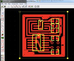
After deciding on the final layout I found Express PCB, a free PCB layout program that has pad layouts for many types of SMD ICs. Using those I could be sure the ICs would fit properly on the traces when I printed them. After laying down the pads for my components I drew out the traces using the line and area drawing tools, which was almost like using MS Paint. (I’ll try to post some of my MS Paint art later. I had mad skillz.)
Etching the PCB
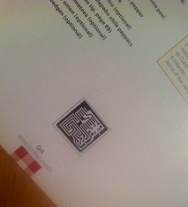
Using
a laser printer I printed the circuit in reverse onto magazine paper.
Laser printer toner melts onto the surface of paper rather than soaking
into the paper, so if you heat it again you can transfer it to another
surface. Taping the printed circuit to the copper clad board I
transferred the toner to the copper using a clothes iron on high.
Once
the copper clad cooled I started removing the paper. Magazine paper is
good to use for this process because it is usually lower quality paper
that starts to fall apart quickly in water. Unfortunately I grabbed a
cooking magazine which actually had fairly high quality and absurdly
water resistant paper. (In hindsight this makes sense because you’ll
likely be cooking with it nearby and you don’t want it falling apart
because you spilled something on it.) I needed to soak the paper and
copper clad in water for probably an hour or two, periodically rubbing a
little bit of paper off very gently.
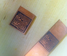
Eventually all the paper fibers were removed and it was ready to be etched. Quite a lot of people use a mixture of Hydrochloric acid and Hydrogen Peroxide to etch copper. Online you can find all sorts of folks claiming its merits over other etchants, including its re-usability. I chose to use it because the local Radio Shack didn’t have etchant on hand and I could get what I needed for this alternative in one trip to the hardware store. Hydrogen peroxide, of course, you can get just about anywhere. Hydrochloric acid (AKA muriatic acid) can be found as a concrete etchant at many hardware stores.
2 parts hydrogen peroxide, 1 part hydrochloric acid. Add the acid second. AAA (Always add acid). Look it up. It’s a thing.
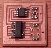
Assembly
After
etching I cleaned the toner off of the piece with acetone. A little
bit a Dremel work to cut the PCB to size and drill the holes and I was
ready to mount the ICs, resistors, and capacitor.
I pulled 6
wires out of an IDE cable to use as a connector cable between my circuit
and the daughter board, soldiering it to the pins on the backside of
the socket where the daughter board connected to the motherboard. The
extra length in the picture was for testing the circuit. Before
connecting the two, the cable was cut off just below the edge of the
daughter board. The fold in the cable allowed me to stretch the cable
out to soldier both ends and then fold it back up between the boards.

After
connecting the boards I used some Testors 1605 Candy Red Transparent
enamel to make my circuit match the original. The enamel is also useful
to avoid oxidation of the copper traces over time since I didn’t tin
the traces. If you use enamel on your PCB make sure it’s
non-conductive. I tested this enable out on some test pieces first.
Anything with metallic flake is likely going to cause you trouble.
To
attach my circuit I used tiny squares of double-sided adhesive foam. I
found it in with the rest of the oddball mounting materials at the
hardware store.

For
the final assembly I remounted the daughter board and attached the old
frayed wires again. Using more wires pulled out of an old IDE cable I
connected my circuit to the power switch and down to a battery mounted
in the fan shroud. Though I could have hidden the battery more if I
removed the SW1 switch from under the power/hdd LEDs and mounted it
there, that would have made changing batteries quite difficult. Instead
I pulled a BIOS battery mount from an old motherboard and ground the
top of the shroud with my Dremel until the holder fit firmly in place. A
dab of epoxy and I now had a completely user-serviceable battery.

This turned out to be a fun little learning experience. Maybe my next PCB will be a little more functional. But, blinking lights…cool, right!?